[ back to Isolation milling WIN ]
Manufacture of printed circuit boards: Isolation milling (isolating conductors)
For a milled PCB isolation, a narrow isolation channel is exposed to the conductors of copper:

Software Isolations milling Sprint Layout ➔ SL2M3 ➔ Mach3 (Website & Programm WIN)
Difference in the chemical process:
Wherein an etched printed circuit board all the not required copper is removed, only the conductor tracks are present:
[ Top of Page ]
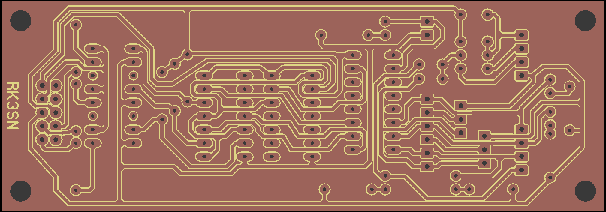
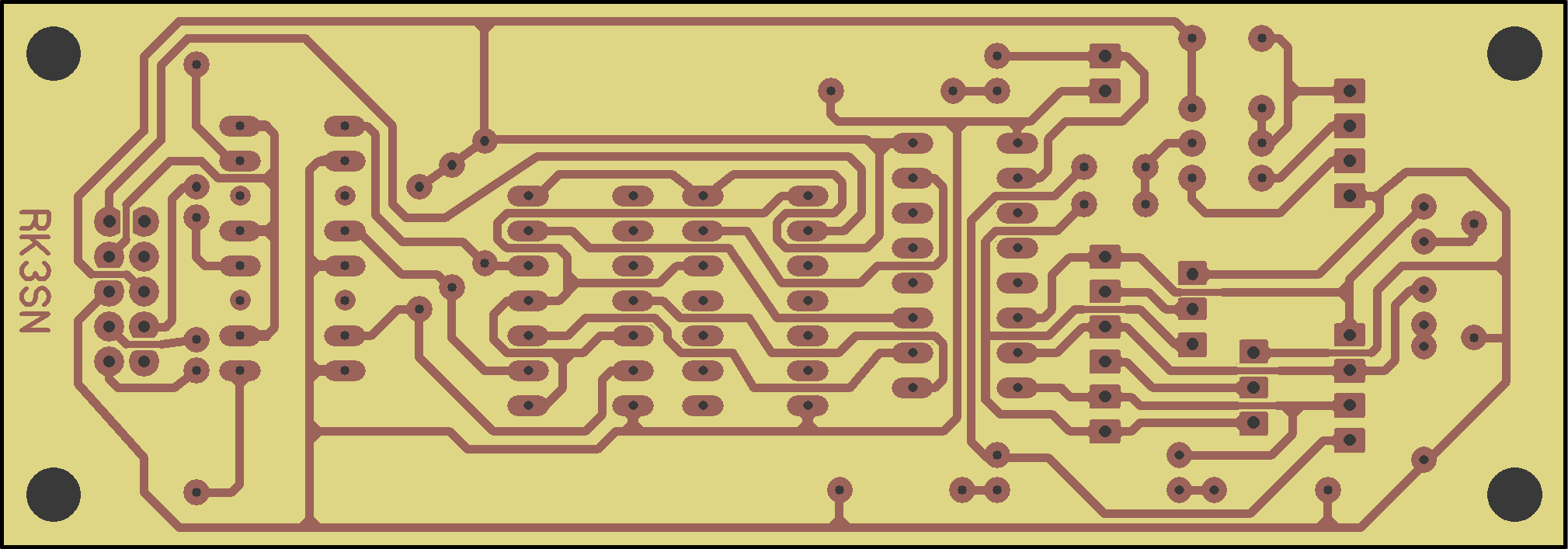
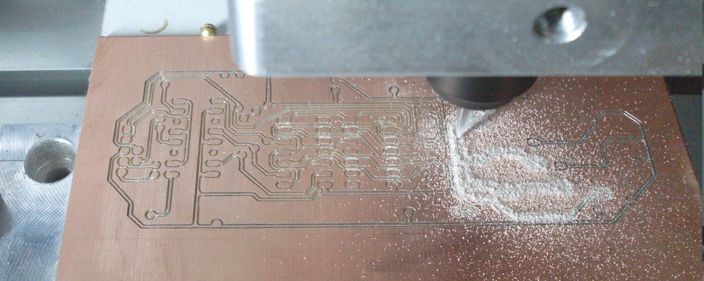
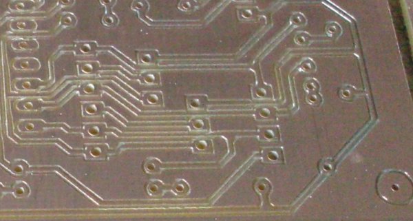
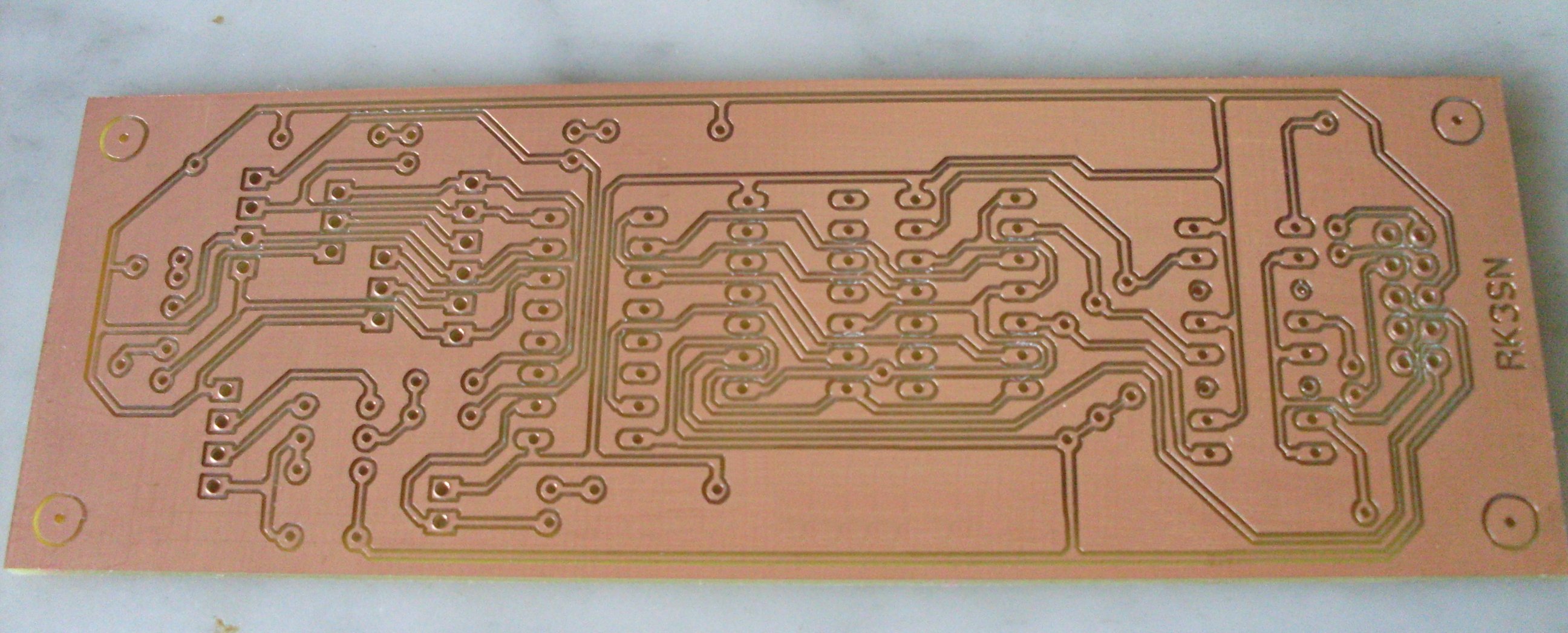
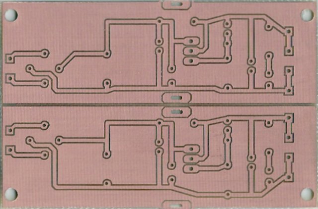
Some images produced by isolation milling of printed circuit boards
Here the milling, isolation routing.
Is then drilled and outline milled.
And done
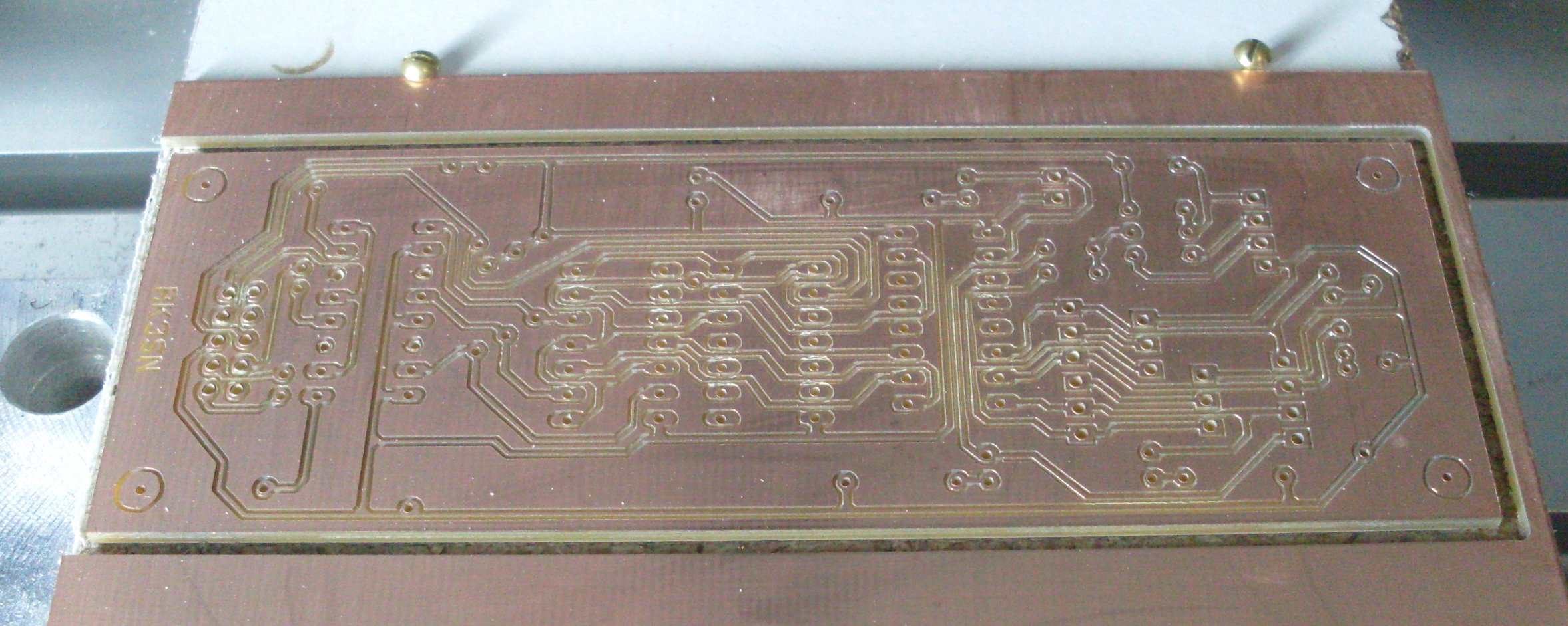
somewhat enlarged
complete view
Fitted from above
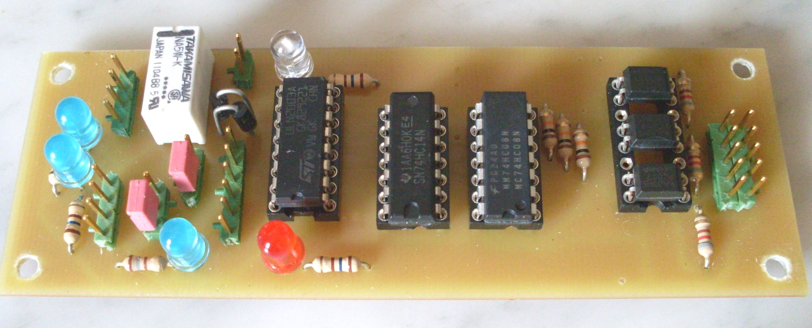
And onother one. As you can see, traces are still possible between two IC contacts (2,54 mm).
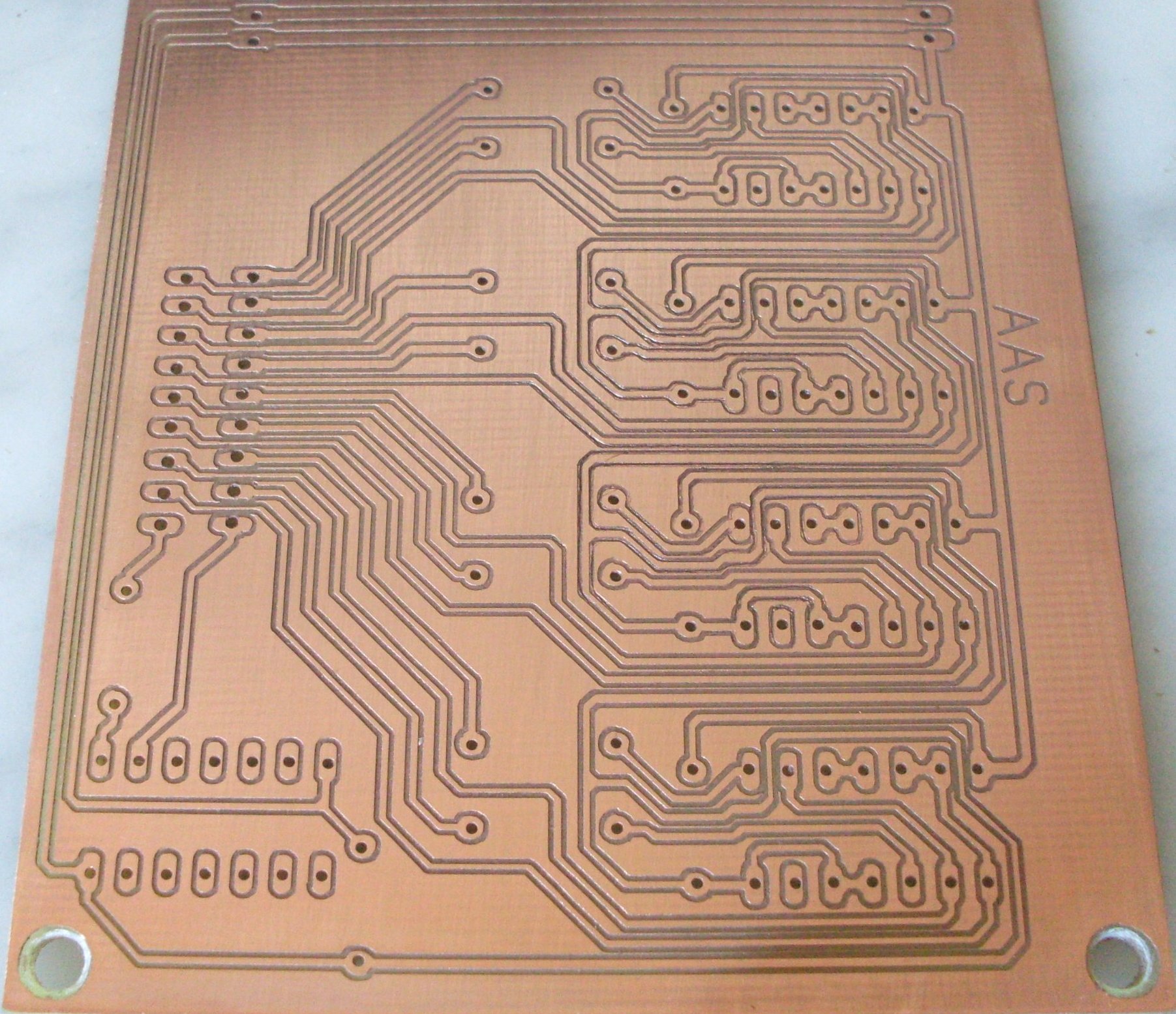
This is a 2-Power Supplies-board, this time scanned. Here were milled slots for the heatsink mounting with equal.
[ Top of Page ]